I spent this week mainly on documenting possible requirements of the serial expansion board in a requirements document and coming up with my first board design.
I started looking for PTZ camera interfaces first. It was quite an overwhelming task to begin with. To be able to decide which interfaces are reasonable to support I went through a lot of PTZ camera programming manuals (which were not easy to dig) and blogs about hacking them. Many of these documents were scanned large pdfs and Ctrl+F didn’t work there. I was also worried about having to support a lot of interfaces. But as I started unifying the interface requirements of major PTZ camera systems I got a sweet result in the end, that most PTZ cameras can be made to work easily with RS232 DB9 port (fig. 1) and RS422 RJ-45 port (fig. 2).
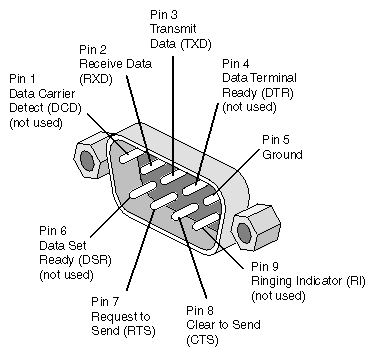 |
Fig 1 |
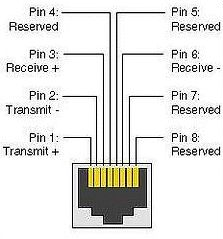 |
| Fig 2 |
Note that the RJ-45 pinout for RS422 is pretty arbitrary and can depend on the camera system. We still have to figure out a pinout to go for when making the RS422 module. We always have the flexibility of modifying pinouts when crimping the RJ-45 plugs to CAT-5 cables.
Take a look the table below that I made for some PTZ camera systems:
Camera system
|
Cabling
|
Connectors required on controller end
|
Sony EVI series
(e.g. Sony EVI-D30)
|
- For RS-232C connections there is a mini DIN-8 VISCA-IN connector at camera side and DB-9 male at controller side.
- For RS-422 connections there is Phoenix connector towards camera side and RJ-45 plug on controller side. CAT-5 cable is used.
|
- RS-232C DB9 male
- RS-422 RJ-45 jack
|
Panasonic AW series

(e.g. Panasonic AW-HE120)
|
- RS422 over CAT-5 with RJ-45 plugs at both ends.
|
- RS-422 RJ-45 jack
|
Canon VC series

(e.g. Canon VC C50i)
|
- Uses a re-configurable multiconnector (something like phoenix connector) on camera side and RS232C DB-9 male on controller side.
- With the Cannon VC EX-3 adapter it can use mini DIN-8 connector like Sony EVI cameras.
|
- RS232C DB-9 male
|
Beyond PTZ
I looked up some other applications like the DMX512 for stage lighting control. I found that DMX512 frames cannot be directly generated by the serial port because they can have very long packets with specific timing requirements of the spaces in between the frames. Serial ports tend to send data in 9-12 bit frames with no control over the spaces between them from software. For the same reason you would never see a serial port being able to communicate using SPI or I2C. Parallel ports in the old days were good in that regard.
Speaking of parallel port we also have the indispensable GPIO module which is quite similar to a parallel port. It could be used to turn on-off LEDs, drive displays, relays, implement low-speed I2C, SPI or maybe DMX512. DMX512 module however, will be a separate module and will not be a part of GPIO because of some mechanical design considerations.
I came up with a modular design to ensure that we use the available serial ports very efficiently and users would have complete freedom to customize their HDMI2USB. On discussing this with Tim today in our weekly progress chat he came up with some cool ideas for attaching these modules to the board.
Board layout
This was the first design from my end:
But this got chucked out because:
- it is more likely to have cables coming from backwards, i.e. the DB9s should be lined up in the bottom side of this diagram.
- it doesn't seem to fit inside the case that Tim is planning to have for HDMI2USB.
Then my second design on the feedback:
This one has all DB9 connectors on one side. Notice how the adapter module would connect to the DB9 ports. Tim wants them to be fitted inside his case and this had some issues which will become clearer on seeing the next diagram:
The red boundary shows the outline of the box. So there are two problems:
- The width of digilent atlys board can practically have only 3 DB9 connectors
- Notice the red arrow in the bottom. Tim wants to have all these adapter boards and customization within the box. So aligning the vacant DB9 connectors would need some kind of extenders. Not very efficient.
So he suggested a third design:
See the notes in the diagram and notice:
- that we have put the VHDCI connector on another side as shown. This allows us to the fit the 6 DB9s in a wide rackmount case.
- we have two DB9 foot prints on the motherboard. The normal DB9s connect to the outer foot-print, but the daughter-boards connect the the inner footprint so that they do not extend beyond the board outline. This keeps everything aligned and doesn’t need us to use DB9 extension PCBs
This looks good and we’re planning to stick with this for now.
Circuit design
I feel it’s reasonable to add more value to this board by adding complete electrical isolation using isolated DC-DC converters and a digital isolator. Isolation protects our FPGA from surge conditions and it also avoids ground loops. Complete electrical isolation requires us to isolate both power and data lines.
The choice of components changed circuit approach several times. This was an iterative process where I formed some requirement then looked for what the available parts are and based on that I updated my requirements until some important parameters got optimized. The important parameters in my case where power efficiency and cost. A few examples:
- I explored a lot of line driver options for RS232 ports and ways of providing isolated power to them. There were also isolated line drivers available but they were expensive and didn’t provide extra power to run modules that we would connect to these board.
- There were also the cheaper +/-9V line drivers which could have been powered using a bipolar supply but the isolated supply turned out to be expensive, also it didn’t give us the +5V isolated supply that we would need for external modules.
- Apart from isolated DC-DC converter modules there were isolated DC-DC converter monolithic ICs that looked appealing at first but they delivered only 33% efficiency at best. This is not good especially if the HDMI2USB design ever goes battery powered where every mW matters.
In the requirements document I also did some worst case power analysis to find out optimum current limiting resistor (fuse) values and I decided to go with a resettable PTC fuse and choosing the one with suitable tripping curve. However some specifications have changed and I will be reviewing that again.
To do
- My plan is to get this requirements document and some spreadsheets ready asap based on new feedback and get Tim to agree on a design so that I can start building on KiCad.
- Hopefully, I should be able to get PCB gerber designs ready this week.
No comments:
Post a Comment