7 Jul 2014

Daily snippet

We're halfway through!

Coagulated and arranged the components on PCB.


I'll ask Rohit to help me verify the VHDCI footprint by taking a printout of this and checking it against the VHDCI connector he has for right fit and correct alignment.

6 Jul 2014

Daily snippet


  • As usual, fixed issues and created components and footprints. Done with CvPcb on all daughterboards. GPIO-25 and LED are remaining.
  • I don't know how useful the LED daughterboard is, knowing that the serial port lines are not bidirectional. Have to ask my mentor.
  • Created daughterboard slot schematic component and daughterboard slot modules that map to each other can can be changed conveniently. The footprint is 90x40 mm


  • Started arranging components on motherboard PCB, here's a peek:

  • Ignore the placement of reddish components, I have just started and have to arrange things nicely :)


5 Jul 2014

Daily snippet

  • Created footprints, completed footprint associations and started a PCB with components laid out for RS232C, RS422, DMX512, GPIO8, IR and MIDI daughterboards.
  • Rough estimate of maximum daughterboard PCB length:
IR daughterboard: 70 mm
DMX512 daughterboard: 75 mm
RS422 daughterboard: 90 mm
GPIO8 daughterboard: 65 mm
RS232 daughterboard: 60 mm
MIDI daughterboard: 70 mm
  • 90 mm seems minimum daughterboard length to have.
  • Will start arranging components on motherboard PCB, with minimum keepout length of 90 mm for daughterboard slots and will see if there is space for setting daughterboard length greater than 90 mm.

4 Jul 2014

Daily snippet


  • After starting with motherboard PCB design, the very next thing that needed to be done was designing the daughterboard slot footprint, which needed me to decide a depth of the daughterboard.
  • I did not have a basis for deciding the depth, so I thought it is necessary to complete the daughterboard schematics and I completed the remaining daughterboard schematics yesterday and fixed a number of issues with existing schematics - 36 commits!
  • MIDI daughterboard schematics are based on this: http://www.personal.kent.edu/~sbirch/Music_Production/MP-II/MIDI/midi_physical_layer.htm
  • I have completed footprint assignments (CvPcb) and laid out components for RS232C daughterboard (PcbNew)

  • I plan to start PCBs for other daughterboards to spread out components and see how much space they would require and decide a depth.
  • After that I'll get back to motherboard schematics.
  • Not sure if the LED daughterboard has a use, since the serial lines are no bidirectional we can't connect LEDs directly. If it's done through a microcontroller we can probably use the GPIO daughterboard instead.

3 Jul 2014

Daily snippet


  • Changed daughterboard pinouts in schematics support PMOD I2C interface.
  • Looked at the possibility of using bidirectional isolators in data isolation stage, but it was ruled out as they were found to be expensive.
  • Re-justified use of data isolation stage in serial expansion motherboard.
  • Created new kicad modules (footprints)
  • Completed footprint association of components on motherboard schematics using CvPcb
  • Verified footprints for components and checked 0603 footprint to be imperial type instead of metric type. Checked datasheets of all components to make sure correct footprint is assigned to them.
  • Made sure only low current (2mA) LEDs are used.
  • Fixed hole dia and added shield pins in VHDCI module
  • Just started with PcbNew, will be creating new module for the daughterboard slot and start laying them out nicely.


1 Jul 2014

Week 6: Time for PCBs!


Motherboard schematics are ready and we’re all set to do the PCBs for motherboard! Last week was spent on organizing the repository, schematics and making various decisions that affected schematics. There is slightly more work to be done on daughterboards schematics and it needs more reviews and fixing.

We began this week by figuring out the best possible autodetection scheme. We discussed about possible use cases for autodetection and how different autodetection schemes would fit into it. First scheme was measuring RC time constant using an I/O pin on the daughterboard. The problem with this scheme was that the RC time-constant measurement using an I/O pin is prone to errors since it depends on logic level thresholds of the I/O pin, which are not clearly documented and their errors are unknown. Slight change in the threshold values can affect our measurement greatly. These thresholds can depend on temperature, VCC, noise and production batch. A reliable way would be measuring the time constant using a voltage comparator and a precision voltage source. But this is the multimeter method and is a bit expensive.

I and Rohit (who’s doing VGA expansion board) settled for I2C EEPROM based detection where each daughterboard will have an inexpensive, pin addressable EEPROM storing ID and configuration data for that daughterboard. The EEPROM slave address gets set on the motherboard, the addresses depend on the slot the daughterboard is connected to.

We were also suggested to take a look on SPI daisy-chaining of EEPROMs, because that would have been the most flexible auto-detection method. I2C based method is addressed based, all EEPROMs with slave address 0 will have expansion board data and EEPROMs with higher address would have module data. If we want to connect more than one expansion board by splitting VHDCI connector, there would be an address conflict in I2C based detection. SPI daisy-chaining would solve that. But it turns out that SPI daisy chaining is not possible for the reasons documented here by Rohit.


I had completed by first run of schematics which got reviewed by Tim. There was a heap of issues with my repository as well as schematics that were fixed one by one.


This week I started the daughterboards and created templates for them. I completed first run of RS232, IR, RS422, GPIO daughterboards. And there are issues with them to solve. It’ll probably take up to a day.

I updated the requirements document to reflect our new decisions. This document never seems to finish because there’s always something new to add or update. As of now there are things to do in that document - like explaining the system diagram I made. The information related to serial communication has become quite fragmented might needs to be more organised. I have to complete the power calculation spreadsheet which will bring out some new limitations and challenges.

Goals for this week:


It seems we need to wind up the hardware part by this week. We need to:
  • Finish daughterboards, get it reviewed.
  • Update requirements document.
  • Start PCB design, get quote from PCB manufacturers.
  • Once again, check and finalize daughterboard depth, motherboard depth and width.
  • (Hopefully) complete the motherboard PCB by this week.
Here’s a peek at the latest schematics as of now, which you may want to compare it with the older ones in last week’s progress report :)


Daily snippet

  • RS422/RS485 daughterboard schematics done.
  • Created a _common folder in repository to store common hierarchical sheets to be shared between daughterboards.
  • Reduced 6 ports to 5 ports in serial expansion board.
  • PIC18F connections almost sorted out with port J left vacant.
  • Implemented the bus design in motherboard schematic.


30 Jun 2014

Daily snippet

- Didn't do much this Sunday
- Today morning RS4XX all sorted and documented and done in schematic
- Lots of things to do today. Some of them - fixing the bus, completing power consumption diagram and spreadsheet, completing schematics and then looking at github issues.

28 Jun 2014

Daily snippet


  • More github repository issues resolved and a few more added to the pile :D
  • Discussed PIC18 USB pin assignments: We shifted around pins to get access to hardware I2Cs, SPIs and UARTs in best possible way. All thanks to Tim and his spreadsheets!
  • While I was making the RS422 daughterboard I noted that the differences between RS422 and RS485 are not that trivial - RS422 have unidirectional lines and support simplex or full-duplex mode. RS485 can have a bidirectional line and is designed for multitap networks. So it can have simplex or half-duplex modes. http://www.ad-net.com.tw/index.php?id=62
  • A really nice guide that differentiates between RS422 and RS485: http://www.diit.unict.it/users/scava/dispense/II/RS485.pdf
  • Figured out that flow control in RS422 and RS485 is not needed which is well explained here: http://en.wikibooks.org/wiki/Serial_Programming/RS-485#Handshaking I like the way handshaking is explained in 2nd sentence.
  • There's RTS flow control which is used only if supported by software. And it doesn't hurt to provide support for RTS control in hardware by giving a jumper option.
  • Another way of flow control which is sometimes built into the converter hardware is called Automatic Send Data Control. In this method a controller within the converter enables the RS485 transmitters *as soon* as it sees data coming from UART TX and shuts off the transmitter so Hi-Z state after a *certain time* of inactivity. The terms "as soon" and "certain time" are critical here and are highly baud-rate dependent. This is baud-rate specific and hence application specific. This is also not a part of any of the EIA-4XX standard and it might be a marketing thing.
  • If the Automatic Send Data Control is needed and the software doesn't support RTS control we can force it in the FPGA or the PIC18F by manipulating RTS. Here's when board auto-detection can be useful.


26 Jun 2014

Daily snippet


  • Some github issues resolved in my repo.
  • Completed remaining daughterboard drawings.
  • Filled up mechanical spreadsheets and end-point usage spreadsheet.
  • Reassigned PIC18F85J94 pins to use the 4 hardware UARTs. Two of the UARTs also share the only 2 available hardware I2C ports, so I2C for daughterboard auto-detection have to be bitbanged.
  • Understood PIC18F85J94 PPS-Lite multiplexer. Learnt using the PIC18F85J94 pin-usage spreadsheet made by Tim and filled it up with new pin assignments.
  • Went through clocking modes for the above. It turns out that it's internal Fast RC clock (FRC) source has at least 0.25% accuracy required by USB 2.0. However, I've also given the choice of putting a crystal.
  • Rearranged file structure of my repo and started daughterboard schematics.

24 Jun 2014

Week 5 summary: All set to start building!


We are close to our milestone of getting the hardware done.This week was exhaustive, spent mostly on formalizing the mechanical specs of the hardware on this spreadsheet, discussing with my mentor on IRC about the implications of intended chassis type on the mechanical specs and completing the first run of motherboard schematics.

The issue of USB endpoints in Cypress FX2LP still remains unresolved, but we have decided to move forward by providing a support for that if it’s feasible by just leaving the VHDCI connector there. No worries if it doesn't work out because we can alternatively use a PIC18F85J94 based USB interface. This particular microcontroller is being planned to be used in the production board, so all the coding done there can be reused in the production board. The PCB would have the provision to populate either VHDCI or the PIC USB interface parts.

Here’s a peek of the motherboard schematics. I kept it hierarchical to make it easy to modify and scale the complexity.


This is the topmost sheet of the motherboard schematic. All the serial expansion functionality has been abstracted from the specifics of the implementation. This allows the serial expansion circuit design to be added like a component to another schematic project. The serial expansion sheet is connected (through labels) in this schematic to Atlys VHDCI as well as PIC18F85J94 based interface. These two interfaces are called data equipment terminal, a common term used in serial communication, which is quite similar to ‘host’ in USB or ‘master’ in SPI/I2C. On the actual PCB assembly, only one of these DTE interfaces would be populated.

The VHDCI sheet:


This sheet handles connector mappings and shield coupling. Going up again and taking a look into the PIC18 USB sheet:


Here we find the microcontroller that is being planned to use in the production board. Also, pads for 8 LEDs and UART header are being given for debugging.

The serial expansion board also integrates full electrical isolation of device side. There’s a power isolation module and data isolation module. The data isolation also performs level-shifting from 3.3V to isolated 5V.


An EEPROM with slave address 0 is connected which contains the expansion board’s ID. This helps the Atlys board to identify that a serial expansion board is connected when the VHDCI interface is used. When the serial expansion board is detected, the logic would scan for higher slave addresses up to 7 to find daughterboards. The daughterboards would share this I2C bus and have differently addressed EEPROMs.

Note that EEPROMs are not electrically isolated from Vcc because they are not electrically connected in anyway to the actual daughterboard circuits.


The power isolator uses ROE-0505S isolated DC-DC conversion module. The fuse is a resettable PTC fuse and LC filter at output stage filters out switching noise.


Data isolation sheet may look confusing, but these are unidirectional digital isolators arranged to give data isolation to 6 serial ports, each having 6 unidirectional signals lines (3 in and 3 out). Post-fix A refers to DTE side and post-fix B refers to daughterboard side.


The above sheet is more interesting that it looks. Here we connect the isolated signals and power line to the daughterboard header (slot), but we can also connect them directly to daughterboard circuits by adding a daughterboard circuit as a hierarchical sheet. This would be useful if a customized serial expansion board need to be designed that comes preloaded with certain daughterboards.

There will be a few more revisions in the above schematic. We may need to find an alternative to I2C EEPROM auto-detection method if that doesn't fit all requirements. My schematic can be found in my repository.

This is all for now, my plans for next week would be:
  • Completing daughter board designs. Get Tim to agree on the schematics.
  • Starting with Motherboard PCB. Change any mechanical specifications if needed, get Tim to review and iterate.
  • Same with the daughterboards. Get production files ready.
  • The requirements documentation is outdated at the moment, it needs *huge* updates.

Daily snippet


  • Motherboard schematic all done and pushed to my repo.
  • Got Tim to create a fork in TimVideos.
  • Looking at the issues in my repository.

22 Jun 2014

Daily snippet


  • Motherboard schematic all sorted out and is almost done
  • Heavy use of hierarchical sheets would make parts of this schematic resusable
  • For example the Numato production board design can add the block of serial expansion just like a component.
  • Customizations by preloading slots with daughterboard circuits (as hierarchical sheets) becomes very easy.

21 Jun 2014

Daily snippet


  • Completed connector placement drawings for daughterboards and listed them on the mechanical design spreadsheet.
  • Completed support pins and header pins placement drawing for daughterboards.
  • Figured out dependency of daughterboard connector placements on chassis parameters and made a side-view diagram on the spreadsheet to document them.
  • Did motherboard layout on the mechanical design spreadsheet to figure out chassis requirements.


20 Jun 2014

19 Jun 2014

Week 4 summary: Speed bumps :(

Last week was spent on forming the functional description of serial expansion board – what features need to be there, what all functionality is reasonable and feasible to add and how they would work together. I had also discussed with my mentor the board’s design, its modularity and how everything will fit inside the chassis. But there was an important question left to explore - how can we implement USB-Serial interface in the most efficient way – which was not an easy question to answer.

This week was all about getting deeper into physical description of serial expansion board with aim to start building PCB design as soon as possible, but a lot of problems and questions came along the way some of which will need us to reconsider the functional description of the serial interface board. And we have been still carrying the same question this week, which by far is most important one – how would the USB serial interface work? What are the maximum no. of serial ports we can support? This has been keeping me from updating a lot of things in the requirements document which are pending, from mechanical specs to component selection.

Our PTZ cameras require hardware flow control. So those seemingly extra pins in the DB-9 connector for RTS/CTS and DTR/DSR pins are indeed needed. Sony cameras use DTR/DSR pins for handshaking and Canon uses RTS/CTS. Handshaking is important in PTZ cameras because the tasks they perform are mechanical (slow) in nature and they can easily miss out commands due to buffer overflow and perform erratically. So the requirement of having handshaking makes our original question even more complex. If that’s not enough, linux does not natively support DTR/DSR handshaking. Also there were a few other questions that I had in mind but I didn’t discuss because I was more occupied with the above issues. These were:
  • Board design width – What is the maximum permissible width of the motherboard?
  • DMX – We have a transmit channel, do we need a receive channel? What kind of devices are to be supported?
  • MIDI – Same question ^
  • IR remote type – IR remote control protocols are not standardized. I need to know what kind of IR remote control the IR receiver is going to be designed for. Or do we need IrDA?

A lot of similar concerns were there for which I found workarounds. Like:
  • What will be the elevation of daughter board?
  • How will the headers fit to the DB9 footprint?
  • How to solve the issue of redundancy of RS232 drivers?
I have answered these and many others in the requirements document for serial expansion board.

We were counting on the Cypress FX2LP USB engine to implement serial ports. USB has 16 endpoints, EP 0 is reserved and the HDMI2USB firmware in Cypress FX2LP uses only EP 1, 2, 4 and 6. I also noticed that the USB allows use to use the same endpoint number for both direction, so the EP 2 and 4 being used for control serial port of HDMI2USB could be integrated into one endpoint. Based on this understanding I assuming 11 free endpoints are there and I was looking forward to implement up to 8 bulk-only virtual serial ports which require only one endpoint no. per serial port if we do not implement hardware flow control.

On reading the Technical Reference Manual which I sadly didn’t find earlier I finally got answer to my question. And the answer was 0! We can’t have extra serial ports at all because it supports only a few endpoints which are 1,2,4,6 and 8. We made a false assumption that the Cypress FX2LP is a USB controller aimed at flexibility. But it’s rather aimed for high speed transfers and it seems to internally combine these end-points to have reduced no. of large endpoints for achieving higher throughput. Cypress FX2LP is not open-source and there is not much known about its internal operation so it cannot be modified to support our needs.
The bottomline
I do not see any way to use Cypress FX2LP for implementing extra serial ports. And there’s no way a custom multiplexed protocol would work without writing a driver for it (and making it support a number of OSes). Neither the serial driver supports any form of multiplexing. We need to iterate on forming the higher level description of serial expansion board.

Here’s what I propose as of now: Let’s use PIC18F being used in production board to implement the USB-Serial interfaces. This brings up some initial questions to ask my from mentor (if he agrees):
Why was that particular chip (PIC18F85J94) chosen?
Do we plan to use a USB Hub to combine the HDMI2USB and PIC18F’s USB?
That MCU supports only 4 USARTs, if we need more then we would have to bitbang serial ports. Will the MCU handle the workload in additional to existing functionality there?

A plenty of discussion is pending on us to overcome issues.

17 Jun 2014

Daily snippet


  • Fiddling today with the FX2LP code I found that EP 6 (isochronous-in) which is used for UVC is double-buffered but it could also be quad-buffered. I configured the configuration bits to use quad-buffering and built the binary. Will be testing out difference in FPS performance. Here's a temporary link to download the binary.
  • The current situation with Cypress FX2LP needs us to significantly change our ways of integrating serial devices to HDMI2USB; the Cypress - FPGA route does not seem to work
  • It seems we will have to implement the serial expansion board as a standalone board using the PIC18F85J94 being planned to be used in production board.
  • It is also advisable to remove the control serial port currently implemented in Cypress FX2LP in order to free up endpoints for UVC A/B preview and HDMI audio input.

16 Jun 2014

Daily snippet

  • Was trying to implement the endpoint changes in the FX2LP firmware but I have a bad news that Cypress FX1/2 let's you access only endpoints no 1,2,4,6,8 where endpoint 1 is a regular endpoint of int/bulk transfer type and 2,4,6,8 are large endpoints with double/triple/quad buffering. No other endpoints!
  • With endpoints 1, 2, 4, 6 already in use, this puts most of our plans about including UVC A/B preview and HDMI audio in trouble.
  • Here is an excerpt from EZ-USB® Technical Reference Manual, pg 87.

  • Don't know whether the other end-points are being used internally to implement multi-buffering or if they had decided to remove them for simplicity. The C code we have is mostly about initialization and USB descriptors other than that its all binary blobs and there's nothing to play with.
  • Here is another diagram from pg 99 to support this

  • If more curious, go though Chapter 8 - Access to endpoint buffers of that document.
  • Linux serial driver does not natively support DTR/DSR flow control but supports RTS/CTS flow control as described here. We can have DPDT switch to connect DTR/DSR to RTS/CTS as a workaround as explained in that article.

15 Jun 2014

Daily snippet


  • Lots of challenges came up when started looking into mechanical considerations and documenting them.
  • Still have to figure out how many ports we can have.
  • Got a nice Appnote from Cypress that explains how serial ports are done in FX2LP.
  • With the new changes in board design this is getting much more complex than thought!

13 Jun 2014

Daily snippet

- It turns out that Sony PTZ cameras need DTR/DSR flow control and Canon PTZ cameras need RTS/CTS flow control.
- There must be ports on the serial expansion board with hardware flow control enabled.
- So these ports would require additional INT IN endpoint apart from BULK IN/OUT.
- Also each of these would require 6 FPGA pins from VHDCI.
- So there is an open question - how about having just 2 or 4 of these flow-controlled ports? And rest of them without flow control?
- A majority of serial devices work without flow control, and even these PTZ cameras may work without flow control at very low baud rate. But I don't have PTZ cameras to test so I wouldn't want to take chances.
- And there is another question left for us. Do CDC ACM drivers support Bulk only CDC ACM serial port, i.e. the ones without INT IN endpoint?
- Flow control is also a concern with the Numato board design, because that also seems to ignore RTS/CTS and DTR/DSR flow control. Only RX, TX is used in the schematics that I was shown. While this would work with RS422 pretty well, it might not work with RS232C based cameras.

12 Jun 2014

Daily snippet


  • I couldn't meet the deadline for getting the spec doc ready, was away whole day.
  • But at night I did some deep investigation on serial and got very interesting results.
  • Recall that an Endpoint has two directions IN (towards host) and OUT (away from host) except when control transfer is used, which is bidirectional. Bulk, Interrupt and Isochronous transfers are unidirectional and a direction needs to be specified in the Endpoint description.
  • EP0 is a control endpoint and doesn't have IN/OUT direction since it's bidirectional
  • We can have BULK IN/BULK OUT on the SAME endpoint number. Search here for the string "two endpoints may have the same endpoint number but opposing data transfer directions".
  • See the three variants of CDC ACM serial devices over here. We want to use a Bulk-only protocol because that's what we have been effectively using. It takes only 1 EP for implementing Bulk-only protocol.
  • Take a look at this spreadsheet based on my lsbusb -v output of HDMI2USB. It also has a tentative plan of how the endpoints can end up for 8 serial expansion ports
  • Currently EP4 and EP6 are used for bulk in and bulk out which is not necessary. An Interrupt IN on EP1 on Cypress FX2LP is also there which is not being used by the FPGA (in usbtop.vhd).
  • We have some cleaning up to do in the Cypress FX2LP. And it seems we can have more serial ports (11 I guess) with space for proposed endpoints for UVC A/B preview and HDMI Audio. Let's have just have up to 8 serial ports and leave remaining end points for other possible uses?
  • Still investigating whether the standard CDC ACM drivers compulsorily requires the INTERRUPT IN endpoint or not.

11 Jun 2014

Week 3 summary: Serial expansion board design

I spent this week mainly on documenting possible requirements of the serial expansion board in a requirements document and coming up with my first board design.


I started looking for PTZ camera interfaces first. It was quite an overwhelming task to begin with. To be able to decide which interfaces are reasonable to support I went through a lot of PTZ camera programming manuals (which were not easy to dig) and blogs about hacking them. Many of these documents were scanned large pdfs and Ctrl+F didn’t work there. I was also worried about having to support a lot of interfaces. But as I started unifying the interface requirements of major PTZ camera systems I got a sweet result in the end, that most PTZ cameras can be made to work easily with RS232 DB9 port (fig. 1) and RS422 RJ-45 port (fig. 2).


Fig 1
Fig 2


Note that the RJ-45 pinout for RS422 is pretty arbitrary and can depend on the camera system. We still have to figure out a pinout to go for when making the RS422 module. We always have the flexibility of modifying pinouts when crimping the RJ-45 plugs to CAT-5 cables.


Take a look the table below that I made for some PTZ camera systems:


Camera system
Cabling
Connectors required on controller end
Sony EVI series
(e.g. Sony EVI-D30)
- For RS-232C connections there is a mini DIN-8 VISCA-IN connector at camera side and DB-9 male at controller side.

- For RS-422 connections there is Phoenix connector towards camera side and RJ-45 plug on controller side. CAT-5 cable is used.
- RS-232C DB9 male

- RS-422 RJ-45 jack
Panasonic AW series
(e.g. Panasonic AW-HE120)
- RS422 over CAT-5 with RJ-45 plugs at both ends.
- RS-422 RJ-45 jack
Canon VC series

(e.g. Canon VC C50i)
- Uses a re-configurable multiconnector (something like phoenix connector) on camera side and RS232C DB-9 male on controller side.

- With the Cannon VC EX-3 adapter it can use mini DIN-8 connector like Sony EVI cameras.
- RS232C DB-9 male


Beyond PTZ


I looked up some other applications like the DMX512 for stage lighting control. I found that DMX512 frames cannot be directly generated by the serial port because they can have very long packets with specific timing requirements of the spaces in between the frames. Serial ports tend to send data in 9-12 bit frames with no control over the spaces between them from software. For the same reason you would never see a serial port being able to communicate using SPI or I2C. Parallel ports in the old days were good in that regard.


Speaking of parallel port we also have the indispensable GPIO module which is quite similar to a parallel port. It could be used to turn on-off LEDs, drive displays, relays, implement low-speed I2C, SPI or maybe DMX512. DMX512 module however, will be a separate module and will not be a part of GPIO because of some mechanical design considerations.


I came up with a modular design to ensure that we use the available serial ports very efficiently and users would have complete freedom to customize their HDMI2USB. On discussing this with Tim today in our weekly progress chat he came up with some cool ideas for attaching these modules to the board.


Board layout
This was the first design from my end:


But this got chucked out because:
  1. it is more likely to have cables coming from backwards, i.e. the DB9s should be lined up in the bottom side of this diagram.
  2. it doesn't seem to fit inside the case that Tim is planning to have for HDMI2USB.


Then my second design on the feedback:


This one has all DB9 connectors on one side. Notice how the adapter module would connect to the DB9 ports. Tim wants them to be fitted inside his case and this had some issues which will become clearer on seeing the next diagram:


The red boundary shows the outline of the box. So there are two problems:
  1. The width of digilent atlys board can practically have only 3 DB9 connectors
  2. Notice the red arrow in the bottom. Tim wants to have all these adapter boards and customization within the box. So aligning the vacant DB9 connectors would need some kind of extenders. Not very efficient.


So he suggested a third design:


See the notes in the diagram and notice:
  1. that we have put the VHDCI connector on another side as shown. This allows us to the fit the 6 DB9s in a wide rackmount case.
  2. we have two DB9 foot prints on the motherboard. The normal DB9s connect to the outer foot-print, but the daughter-boards connect the the inner footprint so that they do not extend beyond the board outline. This keeps everything aligned and doesn’t need us to use DB9 extension PCBs


This looks good and we’re planning to stick with this for now.


Circuit design


I feel it’s reasonable to add more value to this board by adding complete electrical isolation using isolated DC-DC converters and a digital isolator. Isolation protects our FPGA from surge conditions and it also avoids ground loops. Complete electrical isolation requires us to isolate both power and data lines.


The choice of components changed circuit approach several times. This was an iterative process where I formed some requirement then looked for what the available parts are and based on that I updated my requirements until some important parameters got optimized. The important parameters in my case where power efficiency and cost. A few examples:
  • I explored a lot of line driver options for RS232 ports and ways of providing isolated power to them. There were also isolated line drivers available but they were expensive and didn’t provide extra power to run modules that we would connect to these board.
  • There were also the cheaper +/-9V line drivers which could have been powered using a bipolar supply but the isolated supply turned out to be expensive, also it didn’t give us the +5V isolated supply that we would need for external modules.
  • Apart from isolated DC-DC converter modules there were isolated DC-DC converter monolithic ICs that looked appealing at first but they delivered only 33% efficiency at best. This is not good especially if the HDMI2USB design ever goes battery powered where every mW matters.


In the requirements document I also did some worst case power analysis to find out optimum current limiting resistor (fuse) values and I decided to go with a resettable PTC fuse and choosing the one with suitable tripping curve. However some specifications have changed and I will be reviewing that again.


To do


  • My plan is to get this requirements document and some spreadsheets ready asap based on new feedback and get Tim to agree on a design so that I can start building on KiCad.

  • Hopefully, I should be able to get PCB gerber designs ready this week.

7 Jun 2014

Daily snippet - 2x


  • Here is a draft specification document for the serial expansion board. Have to enter board design drawings and circuit design. May be this will end up being the documentation in my repository.
  • It's being decided that the serial expansion would have 6 x RS232C serial ports with DB9 connectors. When other interfaces are required, conversion modules/adapters will be attached. The DB9 connectors also have excellent mechanical stability for connecting these additional adapters. These serial ports could be used directly with VISCA cable or can connect to any other serial device available on internet.
  • To add more value to this board, I'm planing to give complete galvanic isolation instead of ESD chips.
  • These serial ports will lack hardware control because of the way we will be implementing it on the Cypress FX2LP - only Rx and Tx will be there.
  • Some of the serial adapters would be - Serial-GPIO, Serial-RS485. A Serial-DMX adapter can be designed - the protocol is easy, but since a market option is available, will do this only if I run out of things to do. Even RS-232 to RS485 adapters are available to buy, will go through market offerings to see if I need to make one or not.
  • To feed power to the serial-adapters that I would design I might use the RTS line and connect to VU 5V and provide a jumper to disable it. Choice of RTS comes from this.
  • I would also like to have my serial adapters usable with other USB-Serial adapters, in case someone wants to use it that way. To power it I will provide an additional 5V DC jack.

4 Jun 2014

Daily snippet


  • Doing research on the board requirements.
  • There can be lots of different uses of the serial expansion board and I don't feel this board should be rigid in any way.
  • DMX has a lot of variety. There are different standards, I'm finding DMX 512 to be the most popular on internet and even that uses many variants of XLR connectors.
  • I'm thinking of a modular setup with a base board having the VHDCI connector and 6 UART port headers spaced apart appropriately and a family of pluggable modules that connect to these headers and convert UART to interfaces like RS232, RS4xx, DMX 512 (uses XLR connector), GPIO header etc. 
  • This looks more efficient in many ways - User can keep the same base board and keep plugging-in different modules depending on requirements.

3 Jun 2014

Week 2 summary: forming physical specifications

Serial expansion board status:
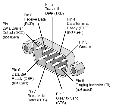
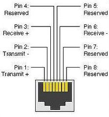
- Decided to keep RJ45, DB9 and DIN8 connectors. RJ45 will be for RS422/485 only. If anyone needs RS232 over RJ45 they may use a DB9 to RJ45 converter cable. The board would get complicated if an option for giving both RS232 and RS485 through RJ-45 has to be provided.

- I will be using separate line-drivers for RS232 and RS485, no SP33x. This gives user an option to populate the components depending on what their camera supports

- To ensure flexibility of choosing VHDCI pins in the serial expansion board, I see the only economical way is to create pads that can be soldered manually through wires.

- Vswt (Unregulated 5V) will be used to power the line-drivers and GPIO header. There will be a fusible resistor to protect the board from overcurrent.

- GPIO header will use an 8-bit bidirectional logic level translator. (Looking for cheapest part that does the job right)

- GPIO header will be 10 pin and will include Ground and 5V supply.

- ESD protectors chosen: GSOT05C (5 will be used near the VHDCI connector)

- Final schematics should be available in 1 or 2 days

VHDL:
- Tried implementing HDMI2USB (master) on Xilinx ISE 14.7 - takes 15 min from synthesize to bitstream on Ubuntu 14.04 LTS (64-bit) and 30 min on my Windows XP (32-bit) VM. My machine has an i5-2520M and 8GB RAM.

- Started reading material on http://www.asic-world.com/vhdl/

Cypress FX2LP:
-From my reading I found that the Cypress chip uses the GPIF interface to send bitstreams to the FPGA during programming mode and uses the endpoint buffers called Slave FIFOs to communicate during normal operation of the device. My concern was mainly to check if the FPGA can access these additional endpoints that I would create and that’s indeed possible by accessing the respective FIFOs in the Cypress chip.

This can be seen in usb_top.vhd:
  constant cdcout : std_logic_vector(1 downto 0):= "00"--ep 2
  constant cdcin  : std_logic_vector(1 downto 0):= "01"--ep 4
  constant uvcin  : std_logic_vector(1 downto 0):= "10"--ep 6

So the task of adding more CDC ACM devices would involve:
· Changing the USB descriptors to describe new interfaces for new CDC ACM devices and their endpoints
· Interfacing the new endpoints to GPIOs in usb_top.vhd

- Revisiting the following diagram (from my proposal) shows a little bit about how the FX2LP is seen as endpoint buffers by the FPGA:


- Just installed their SDK, going through their docs

- Decided on implementing just 2 extra serial ports for now. Procedure for adding more will be documented. Adding more ports dynamically will not be provided in run-time for now.

- Wondering about the driver signing issues I might have in Windows for the custom INFs I will be creating.

Things for coming week:
- Complete the PCB and generate gerber! Will order once we agree on it.

- Look deeper into FX2LP

- Continue my FPGA tutorials